
Solving Dislocation and Stress in Single Crystal Growth
In the manufacturing of III-V compound semiconductors (such as GaAs and InP), minimizing the Etch Pit Density (EPD) is a constant challenge for researchers. When utilizing the Vertical Gradient Freeze process, the interaction between the melt and the container wall is critical. Selecting a reliable VGF crucible is the first step to ensuring high-yield, low-stress crystal synthesis.
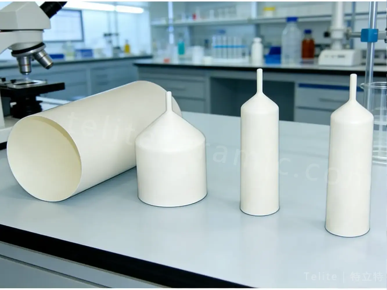
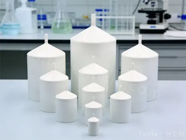
1. Zero Wetting for Stress-Free Demolding
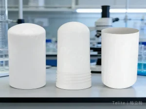
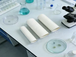
During the VGF process, crystals grow upward from the bottom seed. If the melt adheres to the crucible wall, the differing coefficients of thermal expansion will cause severe internal stress or even crack the crystal during the cooling phase. Upgrading to a Vertical Gradient Freeze crucible made of Pyrolytic Boron Nitride solves this issue. The exceptional non-wetting properties of PBN ensure that the grown crystal simply glides out, completely preventing adhesion-induced dislocations.
2. High Purity to Prevent Polycrystalline Nucleation
Growing single crystals requires maintaining a stable environment at around 1200°C for extended periods. Any impurities released from the container can act as nucleation sites, causing unwanted polycrystalline growth. Telite Ceramics utilizes a Chemical Vapor Deposition (CVD) process to manufacture each pyrolytic boron nitride crucible. With a guaranteed purity of ≥99.99% and zero binders, it provides a perfectly clean environment, making it a highly dependable GaAs crystal growth crucible.
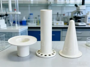
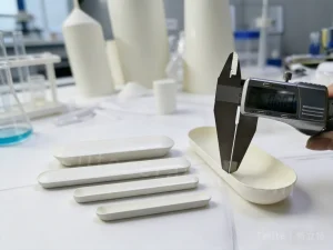
3. Precision Seed Well Machining
The success of the VGF method heavily depends on the precision of the seed well at the bottom of the container. If the well’s inner diameter is too large, the seed crystal will melt; if it is poorly machined, proper thermal contact is lost. Telite Ceramics employs advanced CNC machining to deliver a PBN crystal growth crucible with micrometer-level precision in the seed well area, ensuring perfect compatibility with your specific thermal field.
Customization & RFQ Guide
We provide extensive customization for R&D laboratories and semiconductor production lines. Please Contact Telite Ceramics and provide the following for an accurate quote:
- Crucible dimensions, specifically Seed Well (ID/OD) and taper angles (CAD drawings preferred)
- Operating temperature profile and target material (e.g., GaAs, InP)
- Specific crystal growth furnace compatibility
Technical Director: Engineer Zhang (张工)
Tel / WhatsApp / WeChat: +86-18602175437
Email: telice@teliceramic.com
Xiamen Telite New Material Technology Co., Ltd.

Reviews
There are no reviews yet.