
Advanced PBN Solutions for High-Quality Crystal Growth
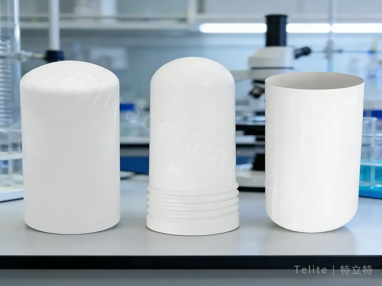
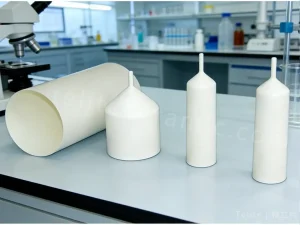
In the synthesis of III-V compound semiconductors (such as GaAs and InP), controlling dislocations and impurities is critical. For the Liquid Encapsulated Czochralski process, the choice of container directly impacts the yield of single crystals. Upgrading to a specialized LEC crucible ensures absolute purity and precise thermal control.
1. Zero Impurity Introduction
During the LEC process, melts reach temperatures well above 1000°C under a B2O3 encapsulant layer. At these extremes, any binder or impurity in the container will leach into the melt, altering the electrical properties of the crystal. By utilizing a binder-free Chemical Vapor Deposition (CVD) process, our pyrolytic boron nitride crucible achieves a purity of ≥99.99%. It guarantees zero outgassing, ensuring your semiconductor crystals remain completely free from external contamination.
2. Preventing Adhesion and Crystal Dislocations
A common cause of high dislocation density is the melt sticking to the crucible wall. As the crystal cools, differences in thermal expansion coefficients create massive internal stress. Fortunately, PBN is highly non-wetting to III-V melts and the B2O3 liquid encapsulant. When using our GaAs crystal growth crucible, the solidified material simply glides against the wall, eliminating cooling stress and resulting in high-quality single crystals.
3. Precise Thermal Gradient Control
The success of a single crystal pull relies heavily on maintaining a stable solid-liquid interface. The unique thermal anisotropy of a PBN crystal growth crucible provides an exceptional advantage. It conducts heat rapidly along the in-plane direction to minimize radial temperature variations, while acting as an insulator in the out-of-plane direction. This specific thermal management provides researchers and equipment manufacturers with the exact temperature gradient required for stable growth.
Customization & RFQ Guide
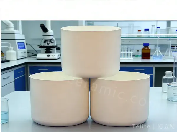
Telite Ceramics supports custom fabrication for R&D institutes and mass production facilities. From internal dimensions and wall thickness to specialized lip designs, we provide precise CNC machining. Please Contact Telite Ceramics with:
- Crucible dimensions (CAD drawings preferred)
- Operating temperature profile and melt material (e.g., GaAs, InP)
- Specific equipment compatibility requirements
Technical Director: Engineer Zhang (张工)
Tel / WhatsApp / WeChat: +86-18602175437
Email: telice@teliceramic.com
Xiamen Telite New Material Technology Co., Ltd.

Reviews
There are no reviews yet.